top of page

Warner Group
Research
Both fundamental and applied research is undertaken in the following areas of Nanostructured Materials with an emphasis on in-situ atomic resolution dynamics of 2D crystals.
-----------------------------------------------------------------
Aberration-corrected transmission electron microscopy and spectroscopy.
Annular dark field scanning transmission electron microscopy (ADF-STEM), 4D STEM with ultrafast pixelated detectors, phase contrast TEM, low voltage single atom TEM (60-80kV), in-situ heating/biasing of 2D materials, atomically resolved electron energy loss spectroscopy (EELS), image simulations based on DFT models.


Materials Chemistry: Synthesis, Functionalization, and Processing
Chemical vapour deposition growth of 2D materials such as graphene, transition metal dichalcogenides and hBN. Nanoscale patterning. Vertical layered heterostructure formation. Interfacing with quantum dots and molecular systems.


Nanoscale Electronic and Opto-electronic Devices
Nanofabricated devices using 2D materials, ultrathin 2D opto-electronics, lateral heterostructures, vertical stacked heterostructures, photodetectors, light emitting devices, flexible electronics, in-situ electrical measurements in the TEM.


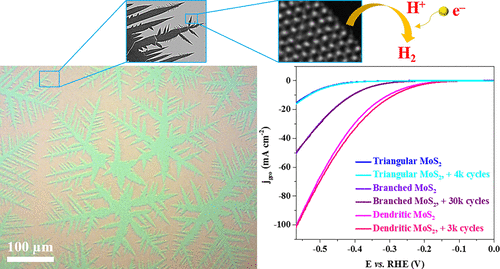
Catalysts and Energy Materials
MoS2 catalyst for hydrogen evolution reaction, Pt doped MoS2, Pt catalysts for fuel cells and HER, Structural analysis of catalyst using TEM.

bottom of page